Lab 6
Analog-to-Digital Conversion
Honor Statement
This is an individual assignment. The code you write, use for the demo and submit should be wholly your own and not produced by working in teams or using, in part or in whole, code written by someone else (found online, from a fellow student, acquaintance, etc.). Penalties for violation include a 0 on the assignment and a potential further deduction or referral to Student Judicial Affairs.
Introduction
In this lab exercise you will learn how to use the Arduino’s analog-to-digital (ADC) conversion capability to interface the microcontroller to a variable resistor, also known as a “potentiometer”, and also to the buttons on the LCD module.
To see a short video demonstrating the operation of lab, click here.
For a copy of the Lab 6 grading sheet, click here
Getting Started
For this lab you will need to get a bag of Lab 6 and 7 components from the instructors. This bag will include the potentiometer used in this lab and some additional parts that will be used in Lab 7.
Set up the Lab 6 assignment the same as has been done previously by creating a lab6 folder in your ee109 folder.
- From the class web site, download the file lab6.zip. This file contains lab6.c, adc.c, adc.h and Lab6_Answers.txt. The adc.c file is a template that will be used in Task 2 to write the code to support the ADC operations.
- Extract the files into the lab6 folder.
- Add a copy of Makefile, lcd.c, lcd.h from a previous lab to the lab6 folder.
- Modify the Makefile to work for the Lab 6 files. It should have
lab6.o,lcd.oandadc.oon the OBJECTS line.
If you look at the lab6.c file you will see that some of the code has been provided for you. At the start of the program add code to do the following:
- Initialize the LCD as has been done in previous labs.
- Put up a splash screen with your name.
Once this has been done you are ready to move on to Task 1 and start adding additional code to interface with some of the hardware.
Task 1: Understanding the ADC
The analog-to-digital conversion module of the Arduino’s microcontroller has the ability to convert an analog voltage to a digital value (a number). In order to do so the ADC must be told what range of voltages to convert to a corresponding range of numbers. The digital range is determined by the number of bits in the resulting numbers. For example, if converting to an 8-bit number, the digital range will be 0 to 255. On the analog side, the ADC must be given two reference voltages, a low reference and a high reference. Any voltage below the low reference will result in a digital value of 0, and any voltage above the high reference results in the maximum digital value. Voltages between the two references are linearly mapped to the numbers between 0 and the maximum value.
The Arduino’s on-chip analog-to-digital converter always uses 0V (GND) as the low voltage reference, but can be configured to use a one of two different high voltage references:
- Use a constant 1.1V source
- Use the 5V (Avcc) power source
For an output, it has two options as to the number of bits in the conversion:
- Generate 8-bit readings (i.e. 2^8 = 256 levels of precision)
- Generate 10-bit readings (i.e. 2^10 = 1024 levels of precision)
Let’s assume the input to the ADC is connected to a voltage source producing 0.8V. For each of the configurations listed below predict the numeric value that the 0.8V input would generate if your Arduino used:
- The 1.1V HIGH reference voltage and 8-bit readings.
- The 5V (Avcc) HIGH reference voltage and 8-bit readings.
- The 1.1V HIGH reference voltage and 10-bit readings.
- The 5V (Avcc) HIGH reference voltage and 10-bit readings.
Now we will confirm these predictions. Use the power supply to generate a constant (DC) voltage of 0.8V and connect it to an open node on your protoboard. Then, use a jumper wire to connect PC1 (A1) of your Arduino to that node on the protoboard.
Open the file adcread.c and examine its contents. The program contains four
functions for reading doing the conversions, one for each of the four cases
described above. In the main part of the program you can uncomment one of these
and leave the other three commented out.
Using the provided Makefile and giving the command make adcread compile and
run the program 4 times, reconfiguring it each time to run through the 4
combinations listed above.
Show your working for the 1.1V HIGH reference voltage and 10-bit reading to a course staff for demo credit.
Task 2: Write the ADC routines
In this task you will finish the code in the adc.c file that is used to
acquire an analog sample and convert it to a digital value. The functions in
this file will be used in this lab and in future labs.
Information on using the ADC module is available in a lecture slide set. A more in-depth review of this material is provided in a separate document “Using the Atmel ATmega328P Analog to Digital Conversion Module available on the class web site. Refer to any of these resources for information on configuring the various registers in the module and how to do the conversions.
The adc.c file contains the template for two routines that you will have to
write.
-
adc_init()- This routine initializes the ADC module. It only needs to be called once at the start of the program but must be called before making any calls to the routine that takes the samples. -
adc_sample()- This routine has one argument, the channel number (0 to 5) to use for the ADC sample. It starts an analog-to-digital conversion on the specified channel, waits for it to complete and then returns the 8-bit result of the conversion to the calling program.
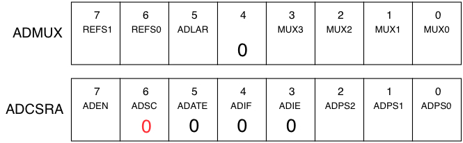
The adc_init routine must set up the proper values in the ADMUX and ADCSRA
registers. Use the information in the ADC lecture slide
set to determine which bits in the
register must be set or cleared by the adc_init function.
Diagrams of the registers are shown below and are also provided on the Lab 6 grading rubric for you to fill in the values.
Important: When writing code to set or clear the bits in these registers by
using the << shift operations, you can use the name of the bit as shown in
the diagram. For example, to set the ADEN bit to a one, the following can be
done.
ADCSRA |= (1 << ADEN)
We strongly encourage you to use the symbolic bit names rather than the 0-7 bit number when doing set/clear/test bit operations.
Your code in adc_init should do the following:
-
Set/clear the REFS[1:0] bits in ADMUX to select the high voltage reference. Using the AVCC reference is appropriate for this lab.
-
Set or clear the ADLAR bit in ADMUX such that we will use 8-bit conversion results (not 10-bit).
-
Set/clear the ADPS[2:0] bits in ADCSRA to select an appropriate prescalar value.
-
Set the ADEN bit in ADCSRA to enable the ADC module.
The channel select bits in ADMUX should not be configured in the adc_init
function. They will be set or cleared each time adc_sample is called
according to the channel argument passed to that function.
The other bits should be left as zeros. The ADSC bit (shown below in red) will
be set to a one in the adc_sample function, but in the initialization of the
registers it should be left unchanged.
The adc_sample routine is called to acquire a sample of the analog signal
from the ADC. The channel to sample is specified as an argument from 0 to 5
when calling the adc_sample routine. The adc_sample routine is declared as a
“unsigned char” function and the return value contains the result of the
conversion and can be saved in an unsigned char variable. For example, to
acquire a sample from ADC channel 2 and put the value in the variable data,
the code would be
data = adc_sample(2);
The adc_sample routine must do the following.
-
Set/clear the MUX[3:0] bits in ADMUX to select the input channel as specified by the argument to the function. The correct bits to go in the MUX[3:0] bits are simply the lower four bits of the argument to the function so just use bit copying to fill these in.
-
Set the ADSC bit in the ADCSRA register to a 1. This starts the conversion process.
-
Enter a loop that tests the ADSC bit each time through the loop and exits the loop when ADSC is 0. This indicates that the conversion is now complete.
-
Copy the 8-bit conversion result from the ADCH register and return it to the calling program.
Once you have finished editing the adc.c file to complete the adc_init and
adc_sample routines, make sure to add adc.o to the OBJECTS line in the
Makefile so it will get compiled when you do a “make” operation. Also make
sure the adc.h file in the same folder with the adc.c.
Task 3: Using the LCD Buttons
The buttons on the LCD use the ADC to determine which, if any, are being pressed. This is different than how buttons in previous labs were interfaced to the Arduino. Rather than having all the LCD buttons produce an individual digital signal, all five of them (UP, DOWN, RIGHT, LEFT and SELECT) are instead interfaced through a multistage voltage divider creating a single analog signal that can be measured by the ADC. Depending on which button is pressed, or none, this circuit produces a different voltage between 0 and 5 volts, and this signal is attached to the ADC Channel 0 input to the Arduino. By using the ADC to convert this voltage to a number it’s easy to determine which if any of the five buttons is pressed.
In order for your program to determine which button was pressed you have to
know what the ADC output is for each button. The easiest way to do that is to
write code to loop continuously reading the ADC result and writing the value to
the LCD. In the following task, we will find out what 8-bit number is returned
by the adc_sample function for each of the five buttons that can be pressed.
These numbers can then be used in your program to determine which button was
pressed.
Open the lab6.c file in your editor and in the top part of the program, add a
call to adc_init to initialize the ADC module and make it ready to take
samples. In the lab6.c there should be a place indicated for this function
call to be added.
Define an “unsigned char” variable to hold the ADC conversion result, and also allocate a “char” buffer of at least 4 characters to use for displaying the value.
In lab6.c look for a while(1) loop that is present in the program just for doing Task 3. This loop is will be used to sample the ADC and print the conversion value on the LCD screen. Add the following code inside this loop.
-
Call
adc_samplewith an argument of zero to read the value of the ADC channel 0 and store the returned value in the variable you define above. -
Use the snprintf routine to format the ADC result into a string of numerical characters that can be displayed. (e.g. something like
snprintf(buf, 5, "%4d", adc_result); -
Use your lcd_moveto function to move the cursor to the first character position on the first row.
-
Use your lcd_stringout function to print the string on the display
Once the program is running, try pressing each button and see what value is displayed. You can record the values shown for each of the buttons on the Lab 6 grading sheet.
Show your results to one of the teaching staff to get checked off for this part of the lab.
You should note that the ADC conversion results may not always be exactly the same each time a button is pressed. Due to electrical noise and thermal effects it may return, for example, 124 one time, 125 another and 126 yet another time. Your code must take this into account when working with the ADC results.
The Variable Resistor
For this lab assignment one of the inputs to the ADC of the Arduino will come from a variable resistor or potentiometer (or “pot” for short) hooked up to be a voltage divider. A potentiometer as shown below is a three-terminal device that has a fixed resistance between two of its wires and a third wire, sometimes called the “slider” that can be adjusted to give anywhere from zero to the full resistance between the slider wire and the other two. In short, the potentiometer operates as a voltage divider (two resistors in series) where the resistance in the numerator can be adjusted by dialing/spinning the “pot”. Turn it fully one direction and you will see 0V on pin 2. Turn it fully in the other direction and you will see VS (5V) on pin 2. At any position in between you should the voltage on pin 2 scale linearly.
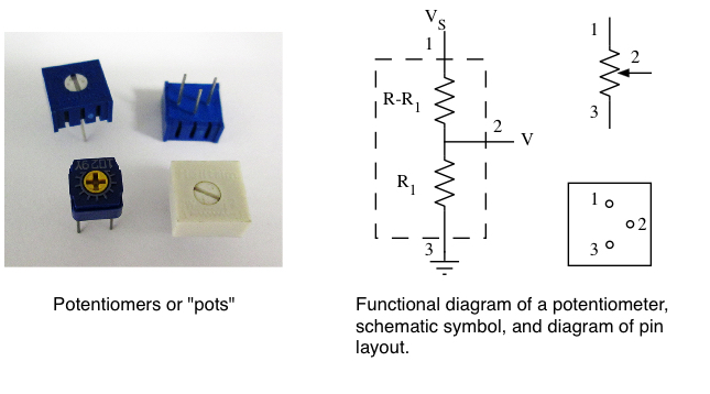
In schematic diagram above of a potentiometer, the total resistance between the top and bottom terminals of the potentiometer is given by R. Internally R can be viewed as two resistors R1 and R-R1 that are in series so the resistance between the top and bottom terminals is fixed at R. Changing the position of the potentiometer’s control changes the resistance of R1. Since the value of R is fixed, as R1 increases, R-R1 must decrease by an equal amount, and similarly if R1 goes down R-R1 must go up.
When hooked up as a voltage divider as above, we can see that V is given by

As the position of the slider is adjusted the value of R1 can change from R (making V=VS) to zero (making V=0). By adjusting the slider we can get any voltage from 0 to V=VS to appear on the slider terminal that will be connected to the ADC input.
Get the potentiometer from the parts provided in your kit and examine it. The resistance between the two fixed terminals (R in the above) is marked on the top next to the round control that is rotated. It should say “102” which is the resistance in the same format as used for marking fixed resistors: 1, 0, and two more zeros = 1000Ω.
Installing the Potentiometer on the Breadboard
In Task 4 below the potentiometer will be used as a variable input to a program running on the Arduino. In this section we will install the potentiometer on the breadboard, connect it to the ADC input of the Arduino and confirm that the analog voltage from the potentiometer is being converted to a digital value. The schematic diagram for this part is shown below.
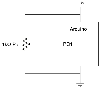
On the potentiometer, the two pins that are on a line parallel to the sides of the device correspond to the top and bottom pins as shown above. The slider pin is the one offset from the other two.
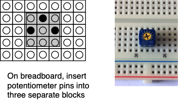
-
Insert the potentiometer into your breadboard so that all three pins are in different 5-hole connection strips as shown below.
-
Using one of the jumpers make a connection from the slider pin’s 5-hole strip to the Arduino A1 (ADC channel 1) input.
-
Using a wire connect one of the other two pins (either one) to the 5V bus on the breadboard.
-
Use a jumper to connect the 5V on the Arduino to the 5V bus on the breadboard.
-
Do the same for ground. Connect a wire from the remaining pin of the potentiometer to the ground bus, and use a jumper to connect ground from the Arduino to the ground bus.
Task 4: Confirm Operation of the Potentiometer
To confirm that you have the potentiometer connected properly, use the multimeter to check that the voltage on the slider pin can be changed by rotating the control.
-
Turn on the DMM and set it for measuring DC volts.
-
Hook the black lead of the DMM to the ground bus of the breadboard, and hook the red lead to the slider pin which is connected to A1.
-
Plug in your Arduino’s USB cable into your computer so there is power to the Ardunio and the Arduino is providing 5V power to the breadboard.
-
Set the DMM to measure DC volts and try rotating the pot with your screwdriver. The indicated voltage should change between +5V and ground as you rotate the pot.
If the voltage is +5V when rotated fully clockwise and 0 when fully counter clockwise, but you want it to be the other way (0 for CW, +5V for CCW), then all you have to do is swap the 5V and ground wires coming from the power and ground buses to the potentiometer and it will now go the other way.
Now that the potentiometer is producing the variable voltage, check to see that
the voltage can be converted by the ADC into a number between 0 and 255. Your
lab6.c file should still have the code to read the ADC value on channel 0 for
the buttons. Change the channel number in the adc_sample function call to
use channel 1 where the potentiometer is connected. Flash the new code to your
Arduino, and then try rotating the potentiometer back and forth.
The program should be displaying the numerical values of its conversions of the voltage on channel 1, and these should be close to 0 at one end of the rotation and close to 255 at the other. If you are not seeing this, you will need to fix the problem before using the potentiometer and ADC code in the next task.
NOTE: The while(1) loop that was used for Task 3 can now be deleted or commented out in your lab6.c file. The while(1) loop that is below that section of the file is the code that will do the rest of the lab assignment.
Task 5: Write a Game Using the ADC
The game you are constructing works in the following manner.
-
The game consist of multiple rounds and when your program starts it will ask how many rounds you want to play. You can use the UP and DOWN buttons on the LCD to change the number. Pressing the SELECT button starts the game operation.
-
At the start of each round the program draws an ‘X’ character at a random position on the first row of the LCD.
-
The position of the potentiometer determines the position of a caret ‘^’ character on the second row. As the potentiometer is turned between the limits of its travel, the ‘^’ should move back and forth between column 0 and column 15 of the second row.
-
When the ‘^’ is positioned under the ‘X’, and left there for two seconds, a message is printed on the screen saying you won the game and that round is over.
-
If there are more rounds to play the next rounds starts.
-
After the last round the program display the total amount of time it took to play all the rounds for the complete game.
Operation of the game
At the start of the game the program should do the following.
-
Initialize both the LCD and the ADC
-
Initialize the random number generation routines. This code is provided for you in the lab6.c file.
-
Display a splashscreen as was done in previous labs identifying which lab this is and showing your name.
-
Each time a new round is started the ‘X’ should be in a different position on the screen. To do this, first use the
rand()function to generate a random number. Each time therand()function is called it returns a number between 0 and 32767 (0x7FFF). Your program should then convert this to a number between 0 and 15 and use that as the initial position of the ‘X’ on the first row. Note: In order to use therand()function, the program must have the line#include <stdio.h>near the top of the program.
Once the above steps have been done the program should enter an infinite loop for the playing of the round. Each time through the loop the following should be done.
-
Use adc_sample to acquire a new 8-bit value for the position of the potentiometer.
-
The 8-bit value must be converted to a column number between 0 and 15. To do this, think about the range of inputs and desired outputs. The ADC produces values 0-255 while we want 0-15. Furthermore, we want consecutive ADC values (as you slowly turn the pot) to produce the same output value. For example ADC value 0,1,2,…,n-1 should all produce output column 0 on the LCD screen for our ‘^’, then n,n+1,n+2…,2n-1 should produce output column 1 on the LCD. Determine n and then think about a simple mathematical operation to convert the input ADC result to the desired output column.
-
If the column number for the ‘^’ has changed, erase the ‘^’ at the old position and draw a new one at the new position.
-
Delay for 10ms
-
Check if the ‘^’ is in the same column as the ‘X’
-
If so, increment a count of how many 10ms intervals it has been there. If the count indicates that it has been there for 2 seconds, print a message that the player has won the round.
-
If not, reset the count to zero. This handles the case where the ‘^’ was under the ‘X’ briefly but then moved on to another column.
-
After a round has been finished the program can start the next round if there are more to play or can enter an infinite loop to stop the game play.
Results
When your program is running you should be able to
-
Turn the potentiometer control back and forth with the screwdriver and see the ‘^’ move smoothly from column 0 to column 15. It should not skip any columns or spend significantly more time on column than another.
-
Move the ‘^’ under the ‘X’ for a time less than 2 seconds several times and the game should not indicate a victory.
-
Move the ‘^’ under the ‘X’ for 2 seconds and the message about winning the game should appear.
Once you have the assignment working demonstrate it to one of the instructors. The answers to the review questions below should be edited into the Lab6_Answers.txt file. The Lab6_Answers.txt file and all source code (lab6.c, adc.c, acd.h, lcd.c, lcd.h, and Makefile) must be uploaded to the Gradescope web site by the due date. See the Assignments page of the class web site for a link for uploading.
Please make sure to save all the parts used in this lab in your project box. These will be needed for labs throughout the rest of the semester. We suggest also saving all the pieces of wire you cut and stripped since those will be useful in later labs.
Review Questions
Answer the following questions and submit them in a separate text file (“Lab6_Answers.txt”) along with your source code.
-
Review the conceptual operation of an ADC and use the given parameters to find the desired value.
- Your 8-bit ADC has Lo and Hi reference voltages of 1V and 4V, what digital number would result from sampling a 2.0V?
- Your 5-bit ADC has Lo and Hi reference voltages of 0V and 5V, what input voltage would yield a digital number of 12?
- Your 6-bit ADC has a Lo reference voltages of 2V. A voltage is sampled at 2.4V and the digital result is 26. What was the Hi reference voltage used by the ADC?
Tammy Trojan has determined that the servo motor can be controlled by TIMER2 even though the PWM period is 16.4ms rather than the preferred 20ms. Billy Bruin also wants to control a similar servo motor but feels it must use a PWM signal with a 20ms period so he will have to use the 16-bit TIMER1 to produce the signal. Note: When TIMER1 is used for PWM, the OCR1A register determines the pulse period, and OCR1B register determines the pulse width. What values will Billy have to use for the TIMER1 prescalar, the OCR1A value to give a 20ms pulse period, and the values for OCR1B to give the minimum pulse width of 0.75ms and the maxumum pulse width of 2.25ms?