EE109 – Spring 2023: Introduction to Embedded Systems
Lab 9
Hardware Datapath Components
Honor Statement
This is an individual assignment. The code you write, use for the demo and submit should be wholly your own and not produced by working in teams or using, in part or in whole, code written by someone else (found online, from a fellow student, acquaintance, etc.). You will be asked to verify this when you submit your code on Vocareum by signing your name in the honor.txt file on Vocareum. Penalties for violation include a 0 on the assignment and a potential further deduction or referral to Student Judicial Affairs.
Introduction
In this lab exercise you will be wiring up a moderately complex digital circuit to control the color and brightness of an LED. The circuit utilizes some of the hardware functional components we have studied in the lectures. This assignment will use a three-color LED (red, green and blue) where the color to be illuminated is selected using the left and right buttons on the LCD. When these buttons are pressed the LCD will indicate which LED color is on and that color will light up. The brightness of the LED is controlled by a pulse-width modulation (PWM) signal that is selected using the up and down keys on the LCD. Each of the three PWM signals that have different duty cycles to control the brightness of the LED. When these buttons are pressed, the LCD will indicate which brightness setting has been selected and adjust the LED illumination accordingly. Unlike previous labs where the PWM signals were generated by the Arduino software, in this lab the signals are created by hardware. The selection of which color of the LED is lit is also controlled by a combination of hardware and software.
This lab uses several new components that were not provided as part of your lab kit. Each of these will be handed out at the start of the lab sesssion.
For a copy of the Lab 9 grading sheet, click here.
Overview of Circuit
A block diagram of the circuit you will be building is shown below. It consist of five components:
- A 4-bit counter that runs continuously generating output signals that will be used to create the PWM signals. The clock signal for the counter is generated by TIMER1 on your Arduino.
- Some combinational logic (NAND gates) that takes the counter outputs as inputs and from these creates three PWM signals with different duty cycles.
- An 8-bit shift register that is loaded from the Arduino and stores the 2-bit selector numbers for the multiplexer and decoder.
- A 4-to-1 multiplexer that is used to select one of the three PWM signals.
- A 2-to-4 decoder that is used to select which of the three LEDs to illuminate with the PWM signal from the multiplexer.
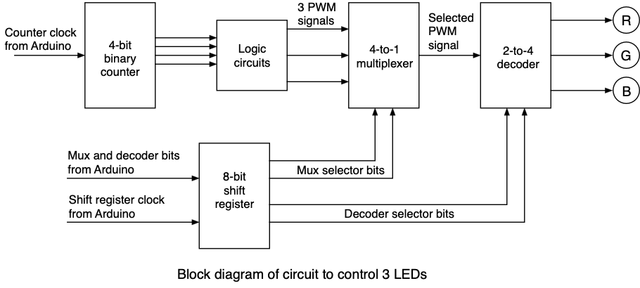
In the sections below we will describe the circuit in more detail including showing how to wire most of it together.
Take care when you start wiring. Some of your demo points are for using APPROPRIATE colors (red = 5V, black = GND) and neatness.
Getting Started
Set up the Lab 9 assignment the same as has been done previously by creating a lab9 folder in your ee109 folder.
- From the class web site, download the file lab9.zip. This file contains lab9.c and Lab9_Answers.txt.
- Extract the files into the lab9 folder.
- Add a copy of Makefile, lcd.c, lcd.h, adc.c and adc.h from a previous lab to the lab9 folder.
- Modify the Makefile to work for the Lab 9 files. It should have
lab9.o,lcd.oandadc.oon the OBJECTS line.
The Lab 9 program will be used during the installation of some of the hardware components so it's necessary to get it running and downloaded to your Arduino before installing most of the hardware. If you look at the lab9.c files you will see that much of the code has been provided for you. At the start of the program add code to do the following:
- Initialize the LCD and ADC routines as has been done in previous labs.
- Configure the DDR bits for outputs on PB4, PC3 and PC5.
- Initialize TIMER1 for the counter clock. A timer1_init routine has been provided to properly set up TIMER1. All you need to do is call this function at the beginning of the program.
- Enable interrupts.
- Put up a splash screen with your name.
Once this has been done download the code to your Arduino so it can be used in the following tasks.
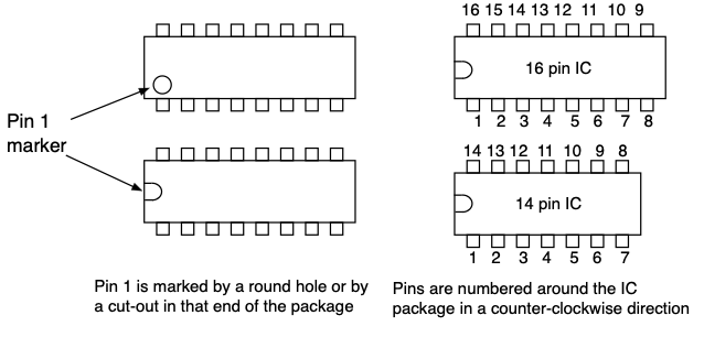
Installing the ICs on the Breadboard
There are five integrated circuits used in this lab. Before installing them on the breadboard make sure that you can identify the proper way to orient the IC. All ICs have a marking on the package to identify pin number 1 as shown below.
There are numerous ways the ICs can be positioned on the breadboard. However the length of the wiring connections that will have to be made can be reduced significantly by careful selection of where to install the ICs. To simplify the wiring connections we strongly recommend that you install the ICs in the positions shown below.
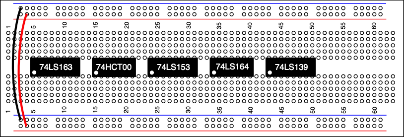
The rows of holes on the breadboard are numbered from 1 to 63 and we recommend installing the ICs so that pin 1 of each IC is in the following positions:
- 5: 74LS163 counter
- 15: 74HCT00 NAND gates
- 24: 74LS153 multiplexer
- 34: 74LS164 shift register
- 43: 74LS139 decoder
The remaining space in rows 51 to 63 will be use for the multicolor LED and associated resistors.
This circuit requires that many of the IC pins be connected to power or ground. To greatly reduce the length of this wiring we strongly recommend installing two wires as shown in the diagram above the that connect the ground bus along the bottom of the board to the ground bus along the top, and similarly for connecting the two power buses together. This will allow you to connect the IC pins to power or ground with very short pieces of wire.
The Circuit, Part 1 - PWM Generation
Note: The following is a description of the first part of the circuit. Don't start wiring it until you have finished reading this section and move to Task 1 in the next section.
The first part of the circuit uses a counter to generate signals that can then be used by combinational logic to generate three PWM signals. The schematic diagram for this part is shown below.
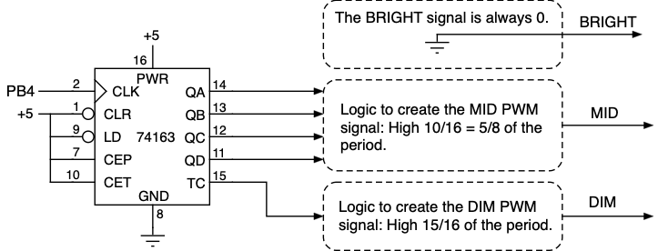
The 4-bit counter is clocked by a 1kHz squarewave signal created by TIMER1 of the Arduino and output on PB4. TIMER1 is configured to generate an interrupt every 0.5msec. Each time the ISR is run it flips the PB4 bit to the opposite state and this creates our 1kHz clock signal.
The 4-bit counter produces five signals (QA, QB, QC, QD and TC) that are inputs to combinational logic circuits that you will have to design. These logic blocks uses the counter outputs to produce three PWM output signals. Note: The LEDs are connected in such a way that they are on when the signal to them is a 0, so a high duty cycle PWM signal will result in a lower intensity LED. The three blocks of combinational logic must do the following.
- For the dimmest setting of the LED, generate a signal that is high 15/16th of the time. This will result in the LED being on 1/16 or 6.25% of the time.
- For the medium setting of the LED, generate a signal that is high 10/16th (= 5/8th) of the time. This will result in the LED being on 6/16th or 37.5% of the time.
- For the brightest setting of the LED, generate a signal that is always in the zero state (i.e. connect this signal to ground). This will result in the LED being on 100% of the time.
Two of the PWM signals require some logic and both can be generated using the four 2-input NAND gates in the 74HCT00 IC included in your parts kit. These will be constructed in the tasks below.
Task 1: Build the Counter and the "DIM" Circuit
For the first part of wiring this lab together we recommend following the steps below to get the counter working and one of the PWM circuits operating
- If you have not done so already download the lab9.c file to the Arduiuno.
- Confirm with a scope that the counter clock signal is being generated on the PB4 output (D12) of the Arduino. It should be a 1kHz squarewave.
- Install the 74LS163 counter IC on the breadboard and make the wiring connections for it as shown in the section above. Make sure to include the power and ground connections.
- Connect the PB4 clock signal to pin 2 of the 74LS163.
- Using the scope observe the QA, QB, QC, QD and TC outputs. QA should be a squarewave at 1/2 the clock frequency, QB is 1/4 the clock, QC is 1/8 the clock, and QD is 1/16 the clock frequency. The TC signal should be high for one period of the PB4 clock when the Q outputs are all 1, and low for the next 15 PB4 clocks.
Now that the counter is working the circuitry can be added to generate the DIM signal from the counter outputs. The DIM signal can be generated from the counter's TC output which is high for one period out of every 16. One of the 2-input NAND gates can be use to invert this signal and the result will be high for 15 clocks our of every 16. Think about how a 2-input NAND gate can be wired to act like an inverter. The 74HCT00 contains four 2-input NAND gates and is shown below. Any of the four gates can be used.

Install the 74HCT00 integrated circuit on the breadboard and make the connections necessary to invert the TC signal to produce the DIM signal. Don't forget to make the power and ground connections to the 74HCT00. Once you have the DIM signal wired, connect the scope to it and confirm that it is low 1/16th of the period and high the rest of the time.
Checkpoint: Show the DIM signal on the scope to a CP to record that you have the checkpoint task completed for this lab. The DIM signal should be low for 1/16 of the period and is being generated from the counter and logic gates.
Task 2: Build the "MID" Circuit
The next part of the lab to work on is designing the combinational logic to generate the "MID" PWM signal.
The "MID" signal needs to be a 1 for 10 of the 16 clock periods before the counter repeats, or 5/8 of the time. To create this signal we recommend doing a 4×4 K-Map with QA, QB, QC and QD as inputs. Pick 10 of the 16 cells to be a 1 that will produce an output that is high for ten consecutive count values and then low for the next six. Grouping the 1's will give a SOP (AND-OR) solution which can be converted to a NAND-NAND circuit. Unfortunately you can't just pick any 10 cells to be 1's. There are two requirements:
- The cells must be consecutive so the signal will be high for 10 clock periods in a row and then low for the next 6 clock periods.
- Remember that you only have three NAND gates left to work with, so the groupings you create on the K-map must be ones that do not need any inverted input signals to implement. If you select the correct 10 cells to be 1's, the resulting SOP logic expression will have no inversions of the input signals.
Once you have the SOP expression for the "MID" circuit convert it from AND-OR form to NAND-NAND form as has been discussed in the lectures. Determine how the three NAND gates will be wired together to implement the signal and make the wiring connections between the counter outputs and the inputs and output of the three remaining NAND gates as needed to implement the "MID" circuit. Once it has been wired up, test it with the scope to see if the signal is doing what is required, being in the 0 state 6/16 or 3/8 of the time.
The Circuit, Part 2 - LED Control
Note: The following is a description of the second part of the circuit. Don't start wiring it until you have finished reading this section and move to Task 3 in the next section.
The second part of the circuit contains the circuitry to control the color and brightness of the illuminated LED. The schematic diagram for this part is shown below
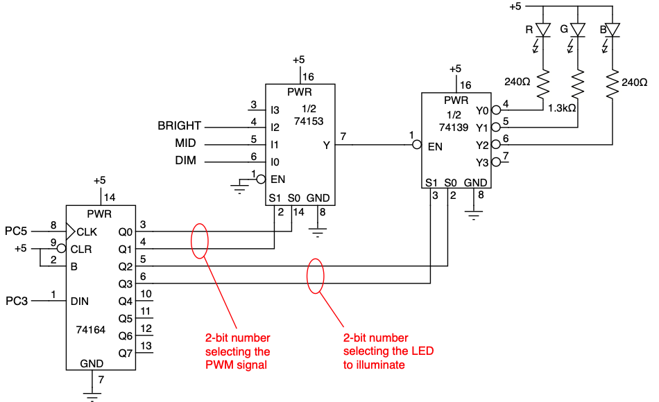
74LS164 Shift Register
The shift register is controlled by two signals from the Arduino.
- PC3 is the data to be stored in the shift register. Your code will have to put the required bit on PC3 before generating the clock signal to load it into the shift register.
- PC5 is the clock signal to store the data on PC3 in the first stage of the shift register (Q0). Your code will have to generate the 0→1→0 signal on PC5 for the clock.
The shift register stores four bits that control the multiplexer and the decoder.
- Bits Q1 and Q0 contain the 2-bit number connected to the S1:S0 multiplexer selector bits for determining which PWM signal is routed to the mux output.
- Bits Q3 and Q2 contain the 2-bit number connected to the S1:S0 decoder selector bits for determining which of the decoder outputs will illuminate the attached LED.
Note that you can not load the individual bits in the shift register. Each time your code needs to change any of the mux or decoder selector bits, it must reload all four bits in the shift register.
74LS153 Dual 4-to-1 Multiplexer
The multiplexer is used to control the LED brightness. This IC contains two 4-to-1 multiplexers but for the lab will only be using one of them. It has the three PWM signals (DIM, MID and BRIGHT) connected to its I0, I1 and I2 inputs. The selector bits (S1 and S0) are connected to the shift register and determine which of these signals appears on the mux output. This will allow selection of which PWM signal reaches the LED and determines how bright it will be.
74LS139 Dual 2-to-4 Decoder/Demultiplexer
The decoder/demultiplexer is used to determine which LED color is illuminated. This IC contains two independent 2-to-4 decoders/demultiplexers. This IC is called a "decoder/demultiplexer" since it can serve either function depending on how it is used. In this lab assignment we will use one of them as a "demultiplexer" (reverse multiplexer). This demultiplexer has active low outputs meaning that the selected output will be in the 0 state and all the other outputs will be in the 1 state. This is the opposite from the decoders that were discussed in the lecture where the selected output was a 1 and all the others were 0. The enable input (EN) is also an active low input so when EN is a 1 this is the disabled state and all the outputs are 1's. We can operate the device as a demultiplexer by connecting the input signal (the PWM signal from the mux) to the EN enable input.
- If EN is a 1, all the outputs are a 1, including the selected one.
- If EN is a 0, the two bits from the shift register determine which of the four demultiplexer output goes to the 0 state.
When used in this manner the PWM signal is effectively connected to whichever output is selected by the two selector bits, essentially a "demultiplexing" operation.
The Y0, Y1 and Y2 outputs from the 74LS139 are connected through current limiting resistors to the three colors of the RGB LED. When the selected decoder output goes to the 0 state, that LED color will illuminate.
Task 3: Build the Shift Register, Mux and Decoder Circuit
In this task we will build the part of the circuit with the shift register, mux and decoder.
- Install the 74LS153, 74LS164 and 74LS139 integrated circuits on the breadboards and make the power and ground connections to them.
- Add any additional connections to power and ground on the three ICs where logic 1 or 0 inputs are required.
- Make the connections between the shift register outputs Q0, Q1, Q2 and Q3 to the mux and decoder S1 and S0 selector bits as shown above.
- Make the connection between the mux output and the decoder EN input.
- Using the jumpers from your lab kit, make the connections for the shift register clock and data from the Arduino PC5 and PC3 outputs.
This completes the installation and wiring of the five integrated circuits. Make sure the wiring is neatly done and the wires are not excessively longer than needed to go between two points.
Task 4: Install the RGB LED
The final component to install on the breadboard is a multicolor LED. These should be available from the table in front of the podium. The LED contains three separate LED elements inside it, one glows red, one glows green and the third glows blue, which leads to them being called "RGB LEDs". The three LEDs inside it have separate cathode (lower voltage) leads, but their anode leads, the one that goes to the higher voltage, are connected together so it is referred to as a "common anode" device. On the package, the common anode lead can be identified since it is longer than the other three. When wiring up an RGB LED, all three elements need to have separate current limiting resistors as shown below.
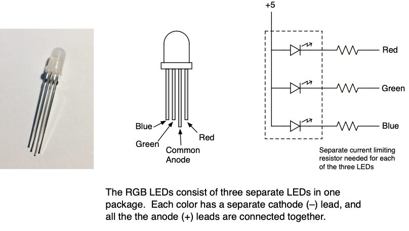
It is recommended that you use the 240Ω resistors from your parts bag for the red and blue LEDs, and use one of the 1.3kΩ resistors for the green LED.
Do the following steps to install the RGB LED.
- Install the LED on the breadboard being careful to have all four leads of the LED in four separate wiring blocks.
- Connect the common anode lead (the longer one) to the +5V bus.
- Connect the three current limiting resistors to the LED red, green and blue leads.
- Connect the other end of the resistors to the decoder outputs as shown on the schematic above. Hint: To make it easier to debug, consider using red wire to connect the red segment, green wire for the green segment, and blue wire for the blue segment.
Task 5: Finishing the Program
The lab9.c file provided for you contains several parts of the program that are already written. All the code for reading the button presses using the ADC and updating the LCD screen is provided and should not have to be modified. This part of the program modifies two variables "level" and "color" to have the values 0, 1 or 2. Whenever either of these variables are changed, the new values must be transmitted to the shift register using two functions that you will have to write (the function skeletons are in the lab9.c file).
shift1bit- This function take a single argument "bit". If the argument is zero, a 0 is shifted into the shift register. If the argument is non-zero, a 1 is shifted into the shift register. This function has to set the proper value on the PC3 output, and then generate the clock pulse on the PC5 output.shift_load- This function is used to load the multiplexer with the selector numbers for the mux and the decoder. This function has two arguments "mux" containing the number from 0 to 2 for the multiplexer selector bits, and "demux" containing the number from 0 to 2 for the decoder/demultiplexer selector bits. Whenevershift_loadis called it must transfer all 4 bits (2 for the mux, 2 for he demux) to the shift register, so it should make four calls to theshift1bitfunction. Theshift_loadfunction must also send the bits in the right order so they end up in the correct positions in the register after all four bits have been clocked into the register.
Write the code for the shift1bit and shift_load functions and you can then test the program to see if it works correctly. Below are some things to test.
- When the left and right buttons are pressed the LED color changes and matches the color indicated on the LCD.
- When the up and down button are pressed the LED brightness changes and should match the level shown on the LCD.
If it is not working correctly, try checking the items below using the scope to observe various signals.
- Check that the shift register bits change as expected when the buttons are used to change the brightness or color settings.
- Check that the mux output changes between the three PWM signals when the up and down buttons are pressed.
- Check that the decoder outputs change when the left and right buttons are pressed to select a color to illuminate.
Results
When your program is running you should be able to confirm the following
- The middle level PWM signal should have a duty cycle of 37.5% (low 3/8 of the period when measured at the LED) as shown on the scope.
- Pressing the left and right buttons changes which color LED is illuminated without changing the brightness of it.
- Pressing the up and down buttons changes the brightness of the LED without changing the color.
- The power and ground wiring should be neatly done using short wires that make the connection from the power and ground buses to the correct pins. See the demo board at the podium for an example.
- The other wiring between the IC pins, resistors and LED should be neatly done and not use excessively long wires.
Once you have the assignment working demonstrate it to one of the instructors. The answers to the review questions below should be edited into the Lab9_Answers.txt file. The Lab9_Answers.txt file and all source code (lab9.c, lcd.c, lcd.h, adc.c, adc.h and Makefile) must be uploaded to the Vocareum web site by the due date. See the Assignments page of the class web site for a link for uploading.
Please make sure to save all the parts used in this lab in your project box. These will be needed for labs throughout the rest of the semester. We suggest also saving all the pieces of wire you cut and stripped since those will be useful in later labs.
Review Questions
Answer the following questions and submit them in a separate text file ("Lab9_Answers.txt") along with your source code.
- Tammy Trojan feels the gap between the MID brightness using a 37.5% PWM signal and the BRIGHT level at 100% is too much and wants to add a fourth brightness level at 75% called "LIT". In our circuit where a low signal turns the LED on this means she needs to create a signal that is low (logic 0) 75% of the time and high (logic 1) 25% of the time. Assuming you had access to additional gates to add to the circuit, how could you create this signal? Write the Boolean logic express for LIT in terms of the output signals from the counter.
- We would like to add a feature where if the Select button is pressed on the LCD, it turns the LED off completely, and then turns it back on when Select is pressed again. Explain how this could be done without having to make any changes to the wiring of the circuit .